TOUCH SCREEN TECHNOLOGIES BASIC INFORMATION AND TUTORIALS


What are the different touch screen technologies?

The first touch-screen was created by adding a transparent surface to a touch-sensitive graphic digitizer, and sizing the digitizer to fit a computer monitor. The initial purpose was to increase the speed at which data could be entered into a computer. Subsequently, several types of touch-screen technologies have emerged, each with its own advantages and disadvantages that may, or may not, make it suitable for any given application.

Resistive Touch-screens
Resistive touch-screens respond to the pressure of a finger, a fingernail, or a stylus. They typically comprise a glass or acrylic base that is coated with electrically conductive and resistive layers. The thin layers are separated by invisible separator dots.

When operating, an electrical current is constantly flowing through the conductive material. In the absence of a touch, the separator dots prevent the conductive layer from making contact with the resistive layer. When pressure is applied to the screen the layers are pressed together, causing a change in the electrical current.

This is detected by the touch-screen controller, which interprets it as a vertical/horizontal coordinate on the screen (x- and y-axes) and registers the appropriate touch event. Resistive type touch-screens are generally the most affordable.

Although clarity is less than with other touch-screen types, they’re durable and able to withstand a variety of harsh environments. This makes them particularly suited for use in POS environments, restaurants, control/automation systems and medical applications.

Infrared Touch-screens
Infrared touch-screens are based on light-beam interruption technology. Instead of placing a layer on the display surface, a frame surrounds it. The frame assembly is comprised of printed wiring boards on which optoelectronics are mounted and concealed behind an IR-transparent bezel.

The bezel shields the optoelectronics from the operating environment while allowing IR beams to pass through. The frame contains light sources (or light-emitting diodes) on one side, and light detectors (or photosensors) on the opposite side.

The effect of this is to create an optical grid across the screen. When any object touches the screen, the invisible light beam is interrupted, causing a drop in the signal received by the photosensors. Based on which photosensors stop receiving the light signals, it is easy to isolate a screen coordinate. Infrared touch systems are solid state technology and have no moving mechanical parts.

As such, they have no physical sensor that can be abraded or worn out with heavy use over time. Furthermore, since they do not require an overlay—which can be broken—they are less vulnerable to vandalism, and are also extremely tolerant of shock and vibration.

Surface Acoustic Wave Technology Touch-screens
Surface Acoustic Wave (SAW) technology is one of the most advanced touch-screen types. The SAW touch-screens work much like their infrared brethren except that sound waves, not light beams, are cast across the screen by transducers. Two sound waves, one emanating from the left of the screen and another from the top, move across the screen’s surface. The waves continually bounce off reflectors located on all sides of the screen until they reach sensors located on the opposite side from where they
originated.

When a finger touches the screen, the waves are absorbed and their rate of travel thus slowed. Since the receivers know how quickly the waves should arrive relative to when they were sent, the resulting delay allows them to determine the x- and y-coordinates of the point of contact and the appropriate touch event to be registered.

Unlike other touch-screen technologies, the z-axis (depth) of the touch event can also be calculated; if the screen is touched with more than usual force, the water in the finger absorbs more of the wave’s energy, thereby delaying it even more.

Because the panel is all glass and there are no layers that can be worn, Surface Acoustic Wave touch screens are highly durable and exhibit excellent clarity characteristics. The technology is recommended for public information kiosks, computer based training, or other high-traffic indoor environments.

Capacitive Touch-screens
Capacitive touch-screens consist of a glass panel with a capacitive (charge storing) material coating on its surface. Unlike resistive touch-screens, where any object can create a touch, they require contact with a bare finger or conductive stylus.

When the screen is touched by an appropriate conductive object, current from each corner of the touch screen is drawn to the point of contact. This causes oscillator circuits located at corners of the screen to vary in frequency depending on where the screen was touched.

The resultant frequency changes are measured to determine the x- and y- coordinates of the touch event. Capacitive type touch-screens are very durable, and have a high clarity. They are used in a wide range of applications, from restaurant and POS use, to industrial controls and information kiosks.


SMART CARD READERS BASIC INFORMATION AND TUTORIALS


What are smart cards?
Instead of fumbling for coins, imagine buying the morning paper using a card charged with small denominations of money. The same card could be used to pay for a ride on public transportation. And after arriving at work, you could use that card to unlock the security door, enter the office, and boot up your PC with your personal configuration.

In fact, everything you purchase, whether direct or through the Internet, would be made possible by the technology in this card. It may seem far-fetched but the rapid advancements of semiconductor technologies make this type of card a reality.

In some parts of the world, the “smart card” has already started to obsolete cash, coins, and multiple cards. An essential part of the smart card system is the card reader, which is used to exchange or transfer information.

Why is the smart card replacing the magnetic strip card?
Because the smart card can hold up to a 100 times more information and data than a traditional magnetic strip card. The smart card is classified as an integrated circuit (IC) card. There are actually two types of IC card—memory cards and smart cards.

Memory cards contain a device that allows the card to store various types of data. However, they do not have the ability to manipulate this data. A typical application for memory type cards is a pre-paid telephone card.

These cards hold typically between 1 KB and 4 KB of data. A memory card becomes a smart card with the addition of a microprocessor. The key advantage of smart cards is that they are easy to use, convenient, and can be used in several applications. They provide benefits to both consumers and merchants in many different industries by making data portable, secure, and convenient to access.

History of Smart Cards
Bull CP8 and Motorola developed the first “smart card” in 1977. It was a two-chip solution consisting of a microcontroller and a memory device. Motorola produced a single chip card called the SPOM 01.

Smart cards have taken off at a phenomenal rate in Europe by replacing traditional credit cards. The key to smart card success has been its ability to authorize transactions off-line. A smart card stores the “charge” of cash, enabling a purchase up to the amount of money stored in the card.

Motorola’s single chip solution was quickly accepted into the French banking system. It served as a means of storing the cardholder’s account number and personal identification numbers (PIN) as well as transaction details. By 1993 the French banking industry completely replaced all bankcards with smart cards.

In 1989 Bull CP8 licensed its smart card technology for use outside the French banking system. The technology was then incorporated into a variety of applications such as Subscriber Identification

Modules (SIM cards) in GSM digital mobile phones. In 1996 the first combined modem/smart card reader was introduced. We will probably soon see the first generation of computers that read smart cards as a standard function.

In May 1996 five major computer companies (IBM, Apple, Oracle, Netscape, and Sun) proposed a standard for a “network computer” designed to interface directly with the Internet, and it has the ability to use smart cards. Also in 1996 the alliance between Hewlett Packard, Informix, and Gemplus was launched to develop and promote the use of smart cards for payment and security on all open networks.

Besides e-commerce, some smart card applications are:
■ Transferring favorite addresses from a PC to a network computer
■ Downloading airline ticket and boarding pass
■ Booking facilities and appointments via Websites
■ Storing log-on information for using any work computer or terminal

THIN FILM TRANSISTOR (TFT) DISPLAYS BASIC INFORMATION AND TUTORIALS


What Are TFT Displays?

Many companies have adopted Thin Film Transistor (TFT) technology to improve color screens. In a TFT screen, also known as active matrix, an extra matrix of transistors is connected to the LCD panel—one transistor for each color (RGB) of each pixel.

These transistors drive the pixels, eliminating the problems of ghosting and slow response speed that afflict non-TFT-LCDs. The result is screen response times of the order of 25 ms, contrast ratios in the region of 200:1 to 400:1, and brightness values between 200 and 250 cd/m2 (candela per square meter).

The liquid crystal elements of each pixel are arranged so that in their normal state (with no voltage applied) the light coming through the passive filter is “incorrectly” polarized and thus blocked. But when a voltage is applied across the liquid crystal elements they twist up to ninety degrees in proportion to the voltage, changing their polarization and letting more light through.

The transistors control the degree of twist and hence the intensity of the red, green, and blue elements of each pixel forming the image on the display. Thin film transistor screens can be made much thinner than LCDs, making them lighter. They also have refresh rates now approaching those of CRTs because current runs about ten times faster in a TFT than in a DSTN screen.

Standard VGA screens need 921,000 transistors (640 x 480 x 3), while a resolution of 1024 x 768 needs 2,359,296, and each transistor must be perfect. The complete matrix of transistors has to be produced on a single, expensive silicon wafer, and the presence of more than a couple of impurities means that the whole wafer must be discarded.

This leads to a high wastage rate and is the main reason for the high price of TFT displays. It’s also the reason why there are liable to be a couple of defective pixels where the transistors have failed in any TFT display.

There are two phenomena that define a defective LCD pixel: a “lit” pixel, which appears as one or several randomly placed red, blue and/or green pixel elements on an all-black background, or a “missing” or “dead” pixel, which appears as a black dot on all-white backgrounds.

The former failure mode is the more common, and is the result of a transistor occasionally shorting in the “on” state and resulting in a permanently “turned-on” (red, green or blue) pixel. Unfortunately, fixing the transistor itself is not possible after assembly. It is possible to disable an offending transistor using a laser.

However, this just creates black dots that would appear on a white background. Permanently turned-on pixels are a fairly common occurrence in LCD manufacturing, and LCD manufacturers set limits, based on user feedback and manufacturing cost data, as to how many defective pixels are acceptable for a given LCD panel.

The goal in setting these limits is to maintain reasonable product pricing while minimizing the degree of user distraction from defective pixels. For example, a 1024 x 768 native resolution panel, containing a total of 2,359,296 (1024 x 768 x 3) pixels, that has 20 defective pixels would have a pixel defect rate of (20/2,359,296)*100 = 0.0008%. The TFT display has undergone significant evolution since the days of the early, twisted Nnematic (TN) technology based panels.

HAND SOLDERING METHOD BASIC INFORMATION AND TUTORIALS


The various soldering methods which are used with electronic assemblies differ in the sequence in which solder, flux, and heat are brought to the joint, and in the way in which the soldering heat is brought to the joint or joints.

With hand soldering, the heat source is the tip of a soldering iron, which is heated to 300–350 °C/570 660 °F. A small amount of flux may have been applied to the joint members before they are placed together.

The assembled joint is heated by placing the tip of the soldering iron on it or close to it. Solder and flux are then applied together, in the form of a hollow solderwire, which carries a core of flux, commonly based on rosin.

The end of the cored wire is placed against the entry into the joint gap. As soon as its temperature has reached about 100 °C/200 °F, the rosin melts and flows out of the solderwire into the joint. Soon afterwards, the joint temperature will have risen above 183 °C/361 °F; the solder begins to melt too, and follows the flux into the joint gap.

As soon as the joint is satisfactorily filled, the soldering iron is lifted clear, and the joint is allowed to solidify. Thus, with hands oldering, the sequence of requirements is as follows:

1. Sometimes, a small amount of flux.
2. Heat, transmitted by conduction.
3. Solder, together with the bulk of the flux.

Clearly, this operation requires skill, a sure hand, and an experienced eye. On the other hand, it carries an in-built quality assurance: until the operator has seen the solder flow into a joint and neatly fill it, he – or more frequently she – will not lift the soldering iron and proceed to the next joint.

Before the advent of the circuit board in the late forties and of mechanized wavesoldering in the mid fifties, this was the only method for putting electronic assemblies together. Uncounted millions of good and reliable joints were made in this way.

Hand soldering is of course still practised daily in the reworking of faulty joints. Mechanized versions of hands oldering in the form of soldering robots have become established to cope with situations, where single joints have to be made in locations other than on a flat circuit board, and which therefore do not fit into a wave soldering or paste-printing routine.

These robots apply a soldering iron together with a metered amount of flux-cored solder wire to joints on three-dimensional assemblies, which because of their geometry do not lend themselves to wave soldering nor to the printing down of solder paste.

Naturally, soldering with a robot demands either a precise spatial reproducibility of the location of the joints, or else complex vision and guidance systems, to target the soldering iron on to the joints.

HISTORY OF FIBER OPTICS IN COMMUNICATION BASIC INFORMATION AND TUTORIALS


How the use of fiber optics in electronic communications developed?

In 1880, only four years after his invention of the telephone, Alexander Graham Bell used light for the transmission of speech. He called his device a Photophone.

It was a tube with a flexible mirror at its end. He spoke down the tube and the sound vibrated the mirror. The modulated light was detected by a photocell placed at a distance of two hundred meters or so. The result was certainly not hi-fi but the speech could at least be understood.

Following the invention of the ruby laser in 1960, the direct use of light for communication was re investigated. However the data links still suffered from the need for an unobstructed path between the sender and the receiver. Nevertheless, it was an interesting idea and in 1983 it was used to send a message, by Morse code, over a distance of 240 km (150 miles) between two mountain tops.

Enormous resources were poured into the search for a material with sufficient clarity to allow the development of an optic fiber to carry the light over long distances.

The early results were disappointing. The losses were such that the light power was halved every three meters along the route. This would reduce the power by a factor of a million over only 60 meters (200 feet).

Obviously this would rule out long distance communications even when using a powerful laser. Within
ten years however, we were using a silica glass with losses comparable with the best copper cables.

The glass used for optic fiber is unbelievably clear. We are used to normal ‘window’ glass looking clear but it is not even on the same planet when compared with the new silica glass. We could construct a pane of glass several kilometers thick and still match the clarity of a normal window.

If water were this clear we would be able to see the bottom of the deepest parts of the ocean. We occasionally use plastic for optic fiber but its losses are still impossibly high for long distance communications but for short links of a few tens of meters it is satisfactory and simple to use.

It is finding increasing applications in hi-fi systems, and in automobile control circuitry. On the other hand, a fiber optic system using a glass fiber is certainly capable of carrying light over long distances.

By converting an input signal into short flashes of light, the optic fiber is able to carry complex information over distances of more than a hundred kilometers without additional amplification. This is at least five times better than the distances attainable using the best copper coaxial cables.

The system is basically very simple: a signal is used to vary, or modulate, the light output of a suitable source — usually a laser or an LED (light emitting diode). The flashes of light travel along the fiber and, at the far end, are converted to an electrical signal by means of a photo-electric cell. Thus the original input signal is recovered.

When telephones were first invented, it took 75 years before we reached a global figure of 50 million subscribers. Television took only 13 years to achieve the same penetration and the Internet passed both in only four years. As all three of these use fiber optics it is therefore not surprising that cables are being laid as fast as possible across all continents and oceans.

Optic fibers carry most of the half million international telephone calls leaving the US everyday and in the UK over 95% of all telephone traffic is carried by fiber. Worldwide, fiber carries 85% of all communications.

PIEZO-ELECTRIC EFFECT BASIC INFORMATION AND TUTORIALS


When electrical stress is applied to one axis of a quartz crystal it exhibits the piezo-electric effect: a mechanical deflection occurs perpendicular to the electric field. Equally, a crystal will produce an e.m.f. across the electrical axis if mechanical stress is applied to the mechanical axis.

If the stress is alternating – the movement of the diaphragm of a crystal microphone is an example – the e.m.f. produced will be alternating at the frequency of the movement. If the stress alternates at a frequency close to the mechanical resonance of the crystal as determined by its dimensions, then large amplitude vibrations result.

Polycrystalline ceramics possess similar qualities. Quartz crystals used for radio applications are slices cut from a large, artificially grown crystal.

The slices are then ground to the appropriate size to vibrate at a desired frequency. The performance of an individual slice – the crystal as the end user knows it – depends upon the angle at which it was cut from the parent crystal.

Each crystal slice will resonate at several frequencies and if the frequency of the stimulus coincides with one of them the output, electrical or mechanical, will be very large.

The vibrations occur in both the longitudinal and shear modes, and at fundamental and harmonic frequencies determined by the crystal dimensions.

Figure 7.1A shows a typical natural quartz crystal. Actual crystals rarely have all of the planes and facets shown.

  
There are three opticalaxes (X, Y and Z) in the crystal used to establish the geometry and locations of various cuts. The actual crystal segments used in RF circuits are sliced out of the main crystal. Some slices are taken along the optical axes, so are called Y-cut, X-cut and Z-cut slabs. Others are taken from various sections, and are given letter designations such as BT, BC, FT, AT and so forth.

MICROWAVE ANTENNA BASIC INFORMATION AND TUTORIALS


What is a microwaves antenna and how to design it?

The small antenna elements at microwaves facilitate the construction of highly directive, high gain antennas with high front-to-back ratios. At frequencies below about 2 GHz, 12- to 24-element

Yagi arrays, enclosed in plastic shrouds for weather protection, may be used. At higher frequencies, antennas with dish reflectors are the norm.

The aperture ratio (diameter/wavelength) of a dish governs both its power gain and beamwidth. The power gain of a parabolic dish is given to a close approximation by:

Gain = 10 log10 6(D/λ)^2 × N, dBi

where D = dish diameter and N = efficiency. Dimensions are in metres. The half-power beam width (HPBW) in degrees is approximately equal to 70λ/D.

A microwave antenna with its dish reflector, or parasitic elements in the case of a Yagi type, is a large structure. Because of the very narrow beamwidths – typically 5◦ for a 1.8m dish at 2 GHz – both the antenna mounting and its supporting structure must be rigid and able to withstand high twisting forces to avoid deflection of the beam in high winds.

Smooth covers, radomes, fitted to dishes and the fibreglass shrouds which are normally integral with Yagis designed for these applications considerably reduce the wind loading and, for some antenna types, increase the survival wind speed.

The electrical performance of a selection of microwave antennas is given in Table 4.1 and the wind survival and deflection characteristics in Table 4.2 (Andrew Antennas, 1991).

Table 4.1 2.1–2.2GHz antennas – electrical characteristics
With shrouded Yagis and some dishes low loss foam-filled cables are generally used up to about 2 GHz although special connectors may be required. At higher frequencies, air-spaced or pressurized nitrogen filled cables are frequently used with waveguides as an alternative.

Table 4.2 Wind survival and deflection characteristics


TYPES OF COAXIAL CABLE BASIC INFORMATION AND TUTORIALS


Coaxial cable consists of two cylindrical conductors sharing the same axis (hence ‘co-axial’) and separated by a dielectric. For low frequencies (in flexible cables) the dielectric may be polyethylene or polyethylene foam, but at higher frequencies Teflon and other materials are used.

Also used in some applications, notably high powered broadcasting transmitters, are dry air and dry nitrogen.

Several forms of coaxial line are available. Flexible coaxial cable discussed earlier in this chapter is perhaps the most common form.

The outer conductor in such cable is made of either braided wire or foil. Again, television broadcast receiver antennas provide an example of such cable from common experience.

Another form of flexible or semi-flexible coaxial line is helical line in which the outer conductor is spiral wound. This type of coaxial cable is usually 2.5 or more centimetres in diameter.

Hardline is coaxial cable that uses a thin-walled pipe as the outer conductor. Some hardline coax used at microwave frequencies has a rigid outer conductor and a solid dielectric.

Gas-filled line is a special case of hardline that is hollow, the centre conductor being supported by a series of thin ceramic or Teflon insulators. The dielectric is either anhydrous (i.e. dry) nitrogen or some other inert gas.

Some flexible microwave coaxial cable uses a solid ‘air-articulated’ dielectric, in which the inner insulator is not continuous around the centre conductor, but rather is ridged. Reduced dielectric losses increase the usefulness of the cable at higher frequencies.

Double shielded coaxial cable provides an extra measure of protection against radiation from the line, and EMI from outside sources from getting into the system.

TRANSMISSION LINE FILTERS, BALUNS AND MATCHING CIRCUITS BASIC INFORMATION AND TUTORIALS


Use can be made of standing waves on sections of line to provide filters and RF transformers. When a line one-quarter wavelength long (aλ/4 stub) is open circuit at the load end, i.e. high impedance, an effective short-circuit is presented to the source at the resonant frequency of the section of line, producing an effective band stop filter.

The same effect would be produced by a short-circuited λ/2 section. Unbalanced co-axial cables with an impedance of 50 ohm are commonly used to connect VHF and UHF base stations to their antennas although the antennas are often of a different impedance and balanced about ground.

To match the antenna to the feeder and to provide a balance to unbalance transformation (known as a balun), sections of co-axial cable are built into the antenna support boom to act as both a balun and an RF transformer.

Balun
The sleeve balun consists of an outer conducting sleeve, one quarter wavelength long at the operating frequency of the antenna, and connected to the outer conductor of the co-axial cable as in Figure 3.5.


When viewed from point Y, the outer conductor of the feeder cable and the sleeve form a short circuited quarter-wavelength stub at the operating frequency and the impedance between the two is very high.

This effectively removes the connection to ground for RF, but not for DC, of the outer conductor of the feeder cable permitting the connection of the balanced antenna to the unbalanced cable without short-circuiting one element of the antenna to ground.

RF transformer
If a transmission line is mismatched to the load variations of voltage and current, and therefore impedance, occur along its length (standing waves). If the line is of the correct length an inversion of the load impedance appears at the input end.

When a λ/4 line is terminated in other than its characteristic impedance an impedance transformation takes place. The impedance at the source is given by:

Zs = Z0^2/ ZL

where
Zs = impedance at input to line
Z0 = characteristic impedance of line
ZL = impedance of load

By inserting a quarter-wavelength section of cable having the correct characteristic impedance in a transmission line an antenna of any impedance can be matched to a standard feeder cable for a particular design frequency.

DOPPLER EFFECT BASIC INFORMATION AND TUTORIALS


What is Doppler Effect?

Doppler effect is an apparent shift of the transmitted frequency which occurs when either the receiver or transmitter is moving. It becomes significant in mobile radio applications towards the higher end of the UHF band and on digitally modulated systems.

When a mobile receiver travels directly towards the transmitter each successive cycle of the wave has less distance to travel before reaching the receiving antenna and, effectively, the received frequency is raised. If the mobile travels away from the transmitter, each successive cycle has a greater distance to travel and the frequency is lowered.

The variation in frequency depends on the frequency of the wave, its propagation velocity and the velocity of the vehicle containing the receiver. In the situation where the velocity of the vehicle is small compared with the velocity of light, the frequency shift when moving directly towards, or away from, the transmitter is given to sufficient accuracy for most purposes by:

fd = V/C fi

where
fd = frequency shift, Hz
ft = transmitted frequency, Hz
V = velocity of vehicle, m/s
C = velocity of light, m/s

Examples are:
• 100 km/hr at 450 MHz, frequency shift = 41.6Hz
• 100 km/hr at 1.8 GHz – personal communication network (PCN)
frequencies – frequency shift = 166.5Hz
• Train at 250 km/hr at 900MHz – a requirement for the GSM pan- European radio-telephone frequency shift = 208 Hz

When the vehicle is travelling at an angle to the transmitter the frequency shift is reduced. It is calculated as above and the result multiplied by the cosine of the angle of travel from the direct approach

In a radar situation Doppler effect occurs on the path to the target and also to the reflected signal so that the above formula is modified to:

fd = V/C fi

where fd is now the total frequency shift.

LOUD SPEAKER AMPLIFIER DAMPING FACTOR BASIC INFORMATION AND TUTORIALS


The majority of high performance amplifiers are solid state and employ global (overall) negative feedback, not least for the unit-to-unit consistency it offers over the wild (eg. +/–50%) tolerances of semiconductor parts. One effect of high global NFB (in conventional topologies) is to make the output source impedance (Zo) very low, potentially 100 times lower than the speaker impedance at the amplifier’s output terminals.

For example, if the amplifier’s output impedance is 40 milliohms, then the nominal damping factor with an 8 ohm speaker will be 200, ie. 40 milliohms (0.04) is 1/200th of 8Ω. This ‘damping factor’ is essential for accurate control of most speakers.

Yet describing an amplifier’s ability to damp a loudspeaker with a single number (called ‘damping factor’) is doubtful. This is true even in active systems where there is no passive crossover with their own energy storage effects, complicating especially dynamic behaviour.

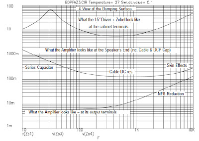
Figure 2.13 again takes a sine-swept impedance of an 8 ohm, 15" driver in a nominal box to show how ‘static’ speaker damping varies. Impedance is 70 ohms at resonance but 5.6 ohms at 450Hz.

  
Now, at the bottom, is plotted the output impedance of a power amplifier which has high negative feedback, and thus the source impedance looking up (or into) it is very low (6 milliohms at 100Hz), though increasing monotonically above 1kHz.

The traditional, simplistic ‘damping factor’ takes this ideal impedance at a nominal point (say 100Hz), then describes attenuation against an 8 ohm resistor. This gives a damping factor of about 3 orders, ie. 1000, but up to 10,000 at 30Hz. Now look at the middle curve: This is what the amplifier’s damping ability is degraded to, after is has traversed a given speaker cable and passed through an ideal 10,000μF series capacitor, as commonly fitted in many professional cabinets for belt’n’braces DC fault protection.

The rise at 1kHz is due to cable resistance, while cable inductance and the series capacitance cause the high and low-end rises respectively above 100 milliohms.

We can easily read off static damping against frequency: At 30Hz, it’s about x100. At mid frequencies, bout x50, and again, about 100 at 10kHz. However, instantaneous dynamic’ impedance may dip four times lower, while the DC resistance portion of the speaker impedance increases after hard drive, recovering over tens to thousands of milliseconds, depending on whether the drive-unit is a tweeter or a 24" shaker.

Even with high NFB, an amplifier’s output impedance will be higher with fewer output transistors, less global feedback, junction heating (if the transistors doing the muscle work are MOS-FETs) and more resistive or inductive (longer/thinner) cabling. Reducing the series DC protection capacitor value so it becomes a passive crossover filter will considerably increase source impedance – even in the pass band.

The ESR (losses) of any series capacitors and inductors will also increase source impedance, with small, but complex, nested variations with drive, temperature, use patterns and aging. The outcome is that the three curves – and the difference between the upper two that is the map of damping factor writhe unpredictably.

Full reality is still more complex, as all loudspeakers comprise a number of complex energy storage/release/exchange sections, some interacting with the room space, and each with the others. The conclusion is that damping factor has more dimensions than one number can convey.

POWER AMPLIFIERS COMMON FORMATS BASIC INFORMATION


Audio power amplifiers are most commonly encountered in one of six formats, which exist to meet real requirements. In order of generally increasing complexity, these are:

1 A monoblock or single channel amplifier. Users are mostly audiophiles who require physical independence as well as implicit electrical isolation (cf.3); or else musicians needing clean, ‘mono’ instrument amplification.

2a A stereo or two channel unit. This is the almost universal configuration. In domestic, recording studio ‘nearfield’ and home studio monitoring use, the application is stereo. For professional studios, and for PA, the two channels may be handling different frequency bands, or the same bands for other speakers, but usually it is the same ‘stereo channel’, as amplifiers are normally behind, over or underneath the L, R or centre speaker cabs they are driving.

2b Dual monoblock – as 2 but the two channels are electrically separated and isolated from each other – the intention being so they can handle vastly different signals without risk of mutual interference. However, being in proximity in a single enclosure and possibly employing a common mains cable, together with having unbalanced inputs, inevitably allows some form of crosstalk through voltage-drop superimposition; and magnetic and/or electrostatic coupling and interaction, between wiring.

3 Multi-channel – most often 3,4 or 6 channels. Originally for professional touring use, for compactness, eventually working within the constraints of the 19" wide ‘rack-mount’ casing system, the de-facto amplifier casing standard for pro audio gear worldwide. Three and six channel mono and stereo ‘Tri-amp’ units have been made so the three frequency bands needed to drive many activelyconfigured PA speakers, can come from a single amplifier box. Multichannel power amps are also applicable to home cinema and home or other installed Ambisonic (higher-dimensional) systems.

4 Integrated power-amp + preamp. Not to be confused with monolithic integrated circuits (ICs), this is the familiar, conventional, budget domestic Hi-Fi ‘amp’. The control functions are built in, saving the cost of a separate pre-amplifier in another box.

But sensitive circuitry (such as high gain disc and tape inputs) may not sit comfortably alongside the stronger AC magnetic fields commonly radiated by power amplifiers’ transformers and supply and output wiring. Careful design is needed to reap cost savings without ending up with irreducible hum and degraded sound quality.

In practice, most integrated amplifiers are built because of a tight budget, and so amplifier performance is traded off in any event. But some high grade examples exist and the trend is increasing at the time of writing.

5 ‘Powered’. The power amp(s) is/are built into the speaker cabinet, to form a ‘Powered’ or ‘Active cabinet’. This approach has been slow to catch on. It has seen some niche use in the past 20 years in smaller installations, and in the home, usually in conjunction with an ‘on-board’ active crossover.

Having one or more amplifiers potentially within inches of the loudspeaker parts they are driving has the clear advantage that the losses, errors and weight in speaker cables are brought down towards the minimum. This is most helpful in large systems where speaker cables are most often at their longest.

Since an amplifier in a speaker cab does not need its own casing, there can be savings in cost, and the total system weight (of amps + speakers) can also be reduced. In the home, the need to live with the conventional amplifier’s bulky metal box is avoided.

One downside, at least for touring, is that even if there is an overall weight reduction, the speaker cabinets assume added weight, which may cause flying (hanging) restrictions. There’s the need to runs mains cables as well as signal cables to each speaker cabinet. This is more of a nuisance in large systems.

For touring sound, health and safety legislation is also unwelcoming to powered cabs, particularly when flown, on several counts. Also, if flown, maintenance can be onerous and adjustment impossible without remote control. Although beyond the remit of this book, it is worth noting that musician’s ‘combo’ amplifiers are an older, simpler and far more widespread variant of the powered cab.

THREE-TERMINAL REGULATOR DESIGN VARIATIONS DIAGRAMS AND TUTORIALS


The following design examples illustrate how 3-terminal regulator integrated circuits can form the basis of higher-current, more complicated designs. Care must be taken, though, because all of the examples render the over temperature protection feature of the 3-terminal regulators useless.

Any overcurrent protection must now be added externally to the integrated circuit. The current-boosted regulator.

The design shown in Figure 2–6 adds just a resistor and a transistor to the 3- terminal regulator to yield a linear regulator that can provide more current to the load.

The current-boosted positive regulator is shown, but the same equations hold for the boosted negative regulator. For the negative regulators, the power transistor changes from a PNP to an NPN. Beware, there is no overcurrent or overtemperature protection in this particular design.

The current-boosted 3-terminal regulator with overcurrent protection This design adds the overcurrent protection externally to the IC. It employs the base-emitter (0.6 V) junction of a transistor to accomplish the overcurrent threshold and gain of the overcurrent stage.

For the negative voltage version of this, all the external transistors change from NPN to PNP and vice versa. These can be seen in Figures 2–7a and b.

Figure 2–6 Current-boosted 3-terminal regulator without overcurrent protection.

Figure 2–7 (a) Positive current-boosted 3-terminal regulator with current limiting. (b) Negative current-boosted 3-terminal regulator with current limiting.


RECOMBINING SEALED LEAD-ACID BATTERIES BASIC INFORMATION AND TUTORIALS


There are two categories of sealed lead-acid cell. These are the non-recombining or partially recombining type, such as those manufactured by Sonnenschein and by Crompton-Parkinson Ltd, and the fully recombining types, as manufactured by the General Electric Company and by the Gates Rubber Company. The fully recombining types are also produced in the UK under licence by Chloride Energy Ltd under the trade name Cyclon.

Particularly towards the end of charge and when being overcharged, the sulphuric acid electrolyte in lead-acid batteries undergoes electrolysis to produce hydrogen and oxygen.

Consequently, in service, the electrolyte level drops and the concentration of sulphuric acid increases, both of which are deleterious to battery performance and, unless attended to by periodic topping up with distilled water, will lead to the eventual destruction of the battery.

Aware of this danger manufacturers recommend a periodic topping up of the electrolyte to the prescribed mark with distilled water. The need for regular topping up has in the past limited the applications in which lead- acid batteries can be used. Manufacturers have adopted two methods of avoiding the need to top up lead-acid batteries:

1. The development of non-recombining or partially recombining batteries in which, by attention to battery design (new lead alloys for grids, etc.) and by using more sophisticated battery charging methods, gassing is reduced to a Aninimum and topping up is avoided.

2. The development of fully recombining types of battenes in which any hydrogen and oxygen produced by gassing is fully recombined to water, thereby avoiding loss of electrolyte volume.

Both methods have been used to produce a range of non-spill either partially or fully recombining sealed lead-acid batteries which are now finding an everincreasing range of applications for this type of battery.

VARIABLE VOLTAGE REGULATOR ELECTRONIC PROJECT DIAGRAM


The variable voltage regulator lets you adjust the output voltage of a fixed dc power supply between 1.2 and 37 V dc, and will supply the output current in excess of 1.5 A. The circuit incorporates an LM117K three terminal adjustable output positive voltage regulator in a TO-3 can.

Thermal overload protection and short circuit current limiting constant with temperature are included in the package. Capacitor C1 reduces sensitivity to input line impedance, and C2 reduces excessive ringing. Diode CR1 prevents C2 from discharging through the IC during an output short.


POWER SUPPLY DESIGN SOFTWARE COMMENT


There is an abundance of software-based power supply design tools, particularly for PWM switching power supply designs. Many of these software packages were written by the semiconductor manufacturers for their own highly integrated switching power supply integrated circuits (ICs).

Many of these ICs include the power devices as well as the control circuitry. These types of software packages should only be used with the targeted products and not for general power supply designs. The designs presented by these manufacturers are optimized for minimum cost, weight, and design time, and the arrangements of any external components are unique to that IC.

There are several generalized switching power supply design software packages available primarily from circuit simulator companies. Caution should be practiced in reviewing all software-based switching power supply design tools.

Designers should compare the results from the software to those obtained manually by executing the appropriate design equations. Such a comparison will enable designers to determine whether the programmer and his or her company really understands the issues surrounding switching power supply design.

Remember, most of the digital world thinks that designing switching power supplies is just a matter of copying schematics.

The software packages may also obscure the amount of latitude a designer has during a power supply design. By making the program as broad in its application as possible, the results may be very conservative.

To the seasoned designer, this is only a first step. He or she knows how to “push” the result to enhance the power supply’s performance in a certain area. All generally applied equations and software results should be viewed as calculated estimates. In short, the software may then lead the designer to a result that works but is not optimum for the system.